Announcement

Collapse
No announcement yet.

What is it that went through the diode to the converter output Capacitor then?

Collapse
X
 
  • Filter
  • Time
  • Show
Clear All
new posts

  • What is it that went through the diode to the converter output Capacitor then?

    I'd like to copy part of Ufopolitics post here to discuss single one topic :

    what is the reason why we can have DC to DC converters or in other words : what is which charges capacitor to the voltage higher then the power source in simple boost converter ?

    Charge Phase
    A basic boost configuration is depicted in Figure 5. Assuming that the switch has been open for a long time and that the voltage drop across the diode is negative, the voltage across the capacitor is equal to the input voltage. When the switch closes, the input voltage, +VIN, is impressed across the inductor and the diode prevents the capacitor from discharging +VOUT to ground. Because the input voltage is DC, current through the inductor rises linearly with time at a rate proportional to the input voltage divided by the inductance.


    Figure 5. Charging phase: when the switch closes, current ramps up through the inductor.

    Discharge Phase
    Figure 6 shows the discharge phase. When the switch opens again, the inductor current continues to flow into the rectification diode to charge the output. As the output voltage rises, the slope of the current, di/dt, though the inductor reverses. The output voltage rises until equilibrium is reached or:

    VL = L × di/dt

    In other words, the higher the inductor voltage, the faster the inductor current drops.

    Figure 6. Discharge phase: when the switch opens, current flows to the load through the rectifying diode.

    In a steady-state operating condition, the average voltage across the inductor over the entire switching cycle is zero. This implies that the average current through the inductor is also in steady state. This is an important rule governing all inductor-based switching topologies.

    The question is : is that the current from inductor which really charges the capacitor or is that only a EMF alone ? You see - the question is so important that it needs answer.
    Last edited by boguslaw; 05-23-2017, 03:59 PM.

  • #2
    Originally posted by boguslaw View Post
    I'd like to copy part of Ufopolitics post here to discuss single one topic :

    what is the reason why we can have DC to DC converters or in other words : what is which charges capacitor to the voltage higher then the power source in simple boost converter ?

    Charge Phase
    A basic boost configuration is depicted in Figure 5. Assuming that the switch has been open for a long time and that the voltage drop across the diode is negative, the voltage across the capacitor is equal to the input voltage. When the switch closes, the input voltage, +VIN, is impressed across the inductor and the diode prevents the capacitor from discharging +VOUT to ground. Because the input voltage is DC, current through the inductor rises linearly with time at a rate proportional to the input voltage divided by the inductance.


    Figure 5. Charging phase: when the switch closes, current ramps up through the inductor.

    Discharge Phase
    Figure 6 shows the discharge phase. When the switch opens again, the inductor current continues to flow into the rectification diode to charge the output. As the output voltage rises, the slope of the current, di/dt, though the inductor reverses. The output voltage rises until equilibrium is reached or:

    VL = L × di/dt

    In other words, the higher the inductor voltage, the faster the inductor current drops.

    Figure 6. Discharge phase: when the switch opens, current flows to the load through the rectifying diode.

    In a steady-state operating condition, the average voltage across the inductor over the entire switching cycle is zero. This implies that the average current through the inductor is also in steady state. This is an important rule governing all inductor-based switching topologies.

    The question is : is that the current from inductor which really charges the capacitor or is that only a EMF alone ? You see - the question is so important that it needs answer.
    Hello Boguslaw,

    I believe I can answer some of your questions, doubts.

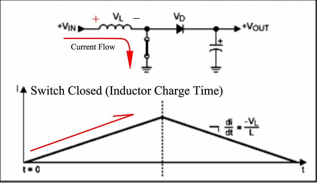
    First let's depict the same images, but showing the Current Flow in the two stages.

    Charge Phase:


    [IMG][/IMG]


    In above Image Switch is CLOSED (Understanding in a real switching device it is a MOSFET)

    When circuit is closed Inductor VL charges up, current flow is depicted by UPPER red arrow.

    Please observe Inductor Polarity above, then realize Diode (VD) will not allow flow through it towards output.

    On lower I/t (Current-Time Graph) note Current Ramping Up shown by Red Arrow.

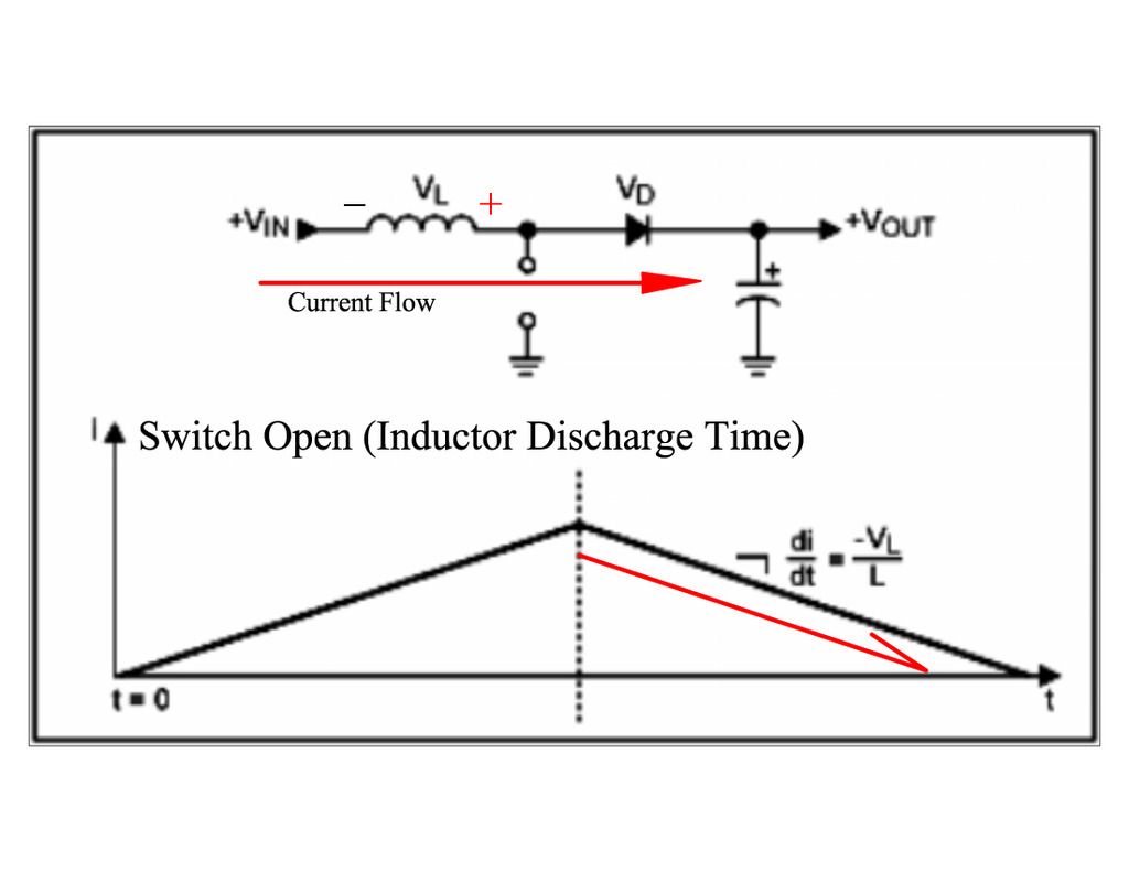
    Discharge Time:

    [IMG][/IMG]

    Above Discharge stage, Switch is Open.

    Note Inductor VL Voltage Polarity swaps.

    Note this swapped voltage polarity on Inductor allows Current Flow through Diode, then to Output Capacitor.

    However, at this stage the Current/Time Graph reflects a Ramp Down Current (red arrow)

    Now resuming your first question:

    Originally posted by boguslaw View Post
    I'd like to copy part of Ufopolitics post here to discuss single one topic :

    what is the reason why we can have DC to DC converters or in other words : what is which charges capacitor to the voltage higher then the power source in simple boost converter ?
    What increases the V Out at end Cap is basically the "Rate of Change" that the switch opens-closes.

    And of course, calculated based on Diode Ultra-Fast Capabilities, plus Inductor Inductance Capabilities...besides switching circuit performance based on the FET Open-Close ratio and response.

    Now your second question:

    Originally posted by boguslaw View Post
    The question is : is that the current from inductor which really charges the capacitor or is that only a EMF alone ? You see - the question is so important that it needs answer.
    I would say is BOTH...Current plus Voltage (or EMF flow as Aaron previously displayed his post on my Thread).

    It is known this Switching Power Supply not only deli8ver Higher Voltage at the end...but also delivers an amperage as a whole "package" correct?

    We would do absolutely nada, nothing by just getting high voltage and zero amps in the output of this DC-DC Converter...right?

    On a side note it was great you decided to open this Thread, since there is more about this same discussion related to Switching Converters...as it gets more complicated whenever we start showing Double Inductor Systems like the SEPIC or

    SINGLE ENDED PRIMARY INDUCTOR CONVERTER


    And...

    The Cúk Converter...


    Regards


    Ufopolitics
    Last edited by Ufopolitics; 05-23-2017, 07:27 PM.
    Principles for the Development of a Complete Mind: Study the science of art. Study the art of science. Develop your senses- especially learn how to see. Realize that everything connects to everything else.― Leonardo da Vinci

    Comment


    • #3
      I propose such experiment to confirm if the inductor is the source of current:


      Zero stage : SW1 closed and capacitor charged mostly to power source voltage V+
      Charge state : SW1 and SW3 closed, SW2 opened
      Discharge state : first SW1 opened then immediately SW3 opened and SW2 closed.

      By such method inductor should discharge directly through the diode to capacitor without being connected to power source.

      If this is a known method the I apologize - I only want to know the results, because I didn't found such experiment described in books.
      Attached Files

      Comment


      • #4
        Nicely done Ufo

        Originally posted by Ufopolitics View Post
        ...
        Discharge Time:

        [IMG][/IMG]

        Above Discharge stage, Switch is Open.

        Note Inductor VL Voltage Polarity swaps.

        Note this swapped voltage polarity on Inductor allows Current Flow through Diode, then to Output Capacitor. ...
        I think it is important to note that in the diagram above, the inductor voltage adds to the input voltage. This is the primary cause of the average capacitor (load) voltage being greater than the input voltage.

        Comment


        • #5
          Ok, zero stage may be modified if the voltage of capacitor after the sequence finishes is not above the power source. In this variant we start with empty capacitor and modify timings to disallow any current from the power source to reach capacitor in any stage.

          Comment


          • #6
            Originally posted by bistander View Post
            I think it is important to note that in the diagram above, the inductor voltage adds to the input voltage. This is the primary cause of the average capacitor (load) voltage being greater than the input voltage.
            Thanks Bistander,

            I agree but not fully on your first sentence above, quoted below:

            "I think it is important to note that in the diagram above, the inductor voltage adds to the input voltage."

            EDIT: Sorry Bistander but did you mean "output voltage" or is it "input voltage"??

            I am answerinbg based on "Output Voltage" below:

            I believe this Voltage discharge from inductor is a very, very short one, I mean it may lasts milli or nano-seconds and it will reflect as a "Hair Pin" (paraphrasing Evostars) Spike...

            I believe the main function of the inductor here is its voltage swapping characteristics which opens-closes Diode Gate to Output...basically, after that function, then serving as a mere wire conductor.

            And so, related to your second sentence:

            "This is the primary cause of the average capacitor (load) voltage being greater than the input voltage."

            Sorry Bi, but I fully disagree with above...IMO the Voltage increase at Output is mainly due to the Frequency level of Repetitions of whole open-close process...a trillion of "Hair Pin spikes" by high frequency repetitions, which is collected and stored at Output Cap.

            But then again, I may be wrong...


            Regards


            Ufopolitics
            Last edited by Ufopolitics; 05-23-2017, 09:52 PM.
            Principles for the Development of a Complete Mind: Study the science of art. Study the art of science. Develop your senses- especially learn how to see. Realize that everything connects to everything else.― Leonardo da Vinci

            Comment


            • #7
              Boost converter

              Ufo,

              When the switch is open:

              V(out) = V(in) + V(L) - V(D)

              That is the mechanism providing the boost (ie. making V(out) higher than V(in). Of course other design considerations must be in line like inductance, capacitance, frequency and duty cycle.

              Regards,

              bi

              Comment


              • #8
                Pulse code modulation allowed some spacing between digital binary.
                The analog is called the flywheel circuit that allows storage between pulses.
                In a closed circuit it is called a buck converter.
                Last edited by mikrovolt; 05-24-2017, 05:53 PM.

                Comment


                • #9
                  Is the voltage increased by the inductor discharging in series with the power source or is it due to the change in pulse timings or both.


                  Edit//// Looks like both, Ill have to learn to type faster. Good info thanks guys.
                  Last edited by lotec; 05-28-2017, 03:45 AM.

                  Comment


                  • #10
                    looking at just relationship of the two components L,C
                    in a parallel circuit and in slow motion, we do some math still
                    it can be as clear as mud. Then you go back to radio shack
                    with more determination and a lot of messing you finally get it to
                    light slowly over 4 seconds. long enough to see it clearly.
                    https://www.youtube.com/watch?v=-GLidgxMr4s

                    Explaining the buck converter correctly it is very important to use the terminology very accurately.
                    In this video the arrows swell up and circuit traces grow longer. Conventional simulation videos using regular arrows
                    can be confusing. Recalling current is the flow of electrical energy and voltage is electrical pressure.
                    https://www.youtube.com/watch?v=vwJYIorz_Aw

                    We can say the inductor exerts a force and we can measure the voltage
                    across the resistor.
                    Last edited by mikrovolt; 05-28-2017, 05:29 AM.

                    Comment


                    • #11
                      microvolt great links, the second one cleared up alot of stuff for me.

                      boguslaw I liked your circuit with the three switches. With the right output voltage sensing being feed back to the right chip controller, I think that you would have both a buck boost(step up), and buck converter(step down) all in one(buck boost converter).

                      When I tried some of these topologies I was a bit disappointed that I was only getting 60% out compared to what I put in, but then I realised that building these circuits around the inductors of motors while they are running the problem was that the inductance would change as it passed a magnet, making them hard to tune. When I tried static inductors they worked alot better. I still think that certain typrs of motors could be ok for that kind of recovery.

                      Comment


                      • #12
                        What I believe for the most part. that goes thru the diode to the load, is a copy of the input power. And the input power is sunk to ground, give or take, depending on the topology and their variations.

                        Regulated Buck Boost circuits might be usable for even more efficient circuits. If the primary current isnt sunk to ground but instead, used to charge a couple of ultracaps (banked juice), as the caps charge up, the potential difference across the input would go down, but the output would be held at the desired voltage level. Once the caps reached a little over one half of the required output voltage, they could be discharged in series across the load, So the load could run off sometimes banked juice and sometimes copied juice.

                        The ultra caps should be big, perhaps say 10 Farads per amp of input, or at least big enough to provide a low impedance path for primary current and take maybe 30 seconds to a minute to charge up to half of output voltage.

                        Comment


                        • #13
                          Smps

                          Modern buck, boost, forward converters and switch mode power supplies run at kilohertz to megahertz frequencies. They can achieve 99% power efficiency. Capacitor sizing is on the mS or uS time constant scales, not minutes.

                          Comment


                          • #14
                            When I was talking about the capacitors, I wasnt referring to input or output capacitors. They are sized well and I dont recommend changing them.

                            I was meaning some boost circuits sink a pulse to ground, in order to harvest what comes off the collapsing magnetic field at a higher voltage. I was thinking that these pulses could be used to charge very large ultra caps. When the ultracaps are at just over one half the wanted output voltage, The boost circuit is shut down temporarily and the two ultra caps are switched in to power the load in series.

                            A circuit that alternates between these two modes of operation has added complexity but may be worth it. The idea is that pulses sunk to ground can be saved and used as well.

                            Comment


                            • #15
                              Charge phase

                              Originally posted by lotec View Post
                              When I was talking about the capacitors, I wasnt referring to input or output capacitors. They are sized well and I dont recommend changing them.

                              I was meaning some boost circuits sink a pulse to ground, in order to harvest what comes off the collapsing magnetic field at a higher voltage. I was thinking that these pulses could be used to charge very large ultra caps. When the ultracaps are at just over one half the wanted output voltage, The boost circuit is shut down temporarily and the two ultra caps are switched in to power the load in series.

                              A circuit that alternates between these two modes of operation has added complexity but may be worth it. The idea is that pulses sunk to ground can be saved and used as well.
                              Hi Iotec,

                              I assume you're referring to this portion of the cycle (red arrow).

                              Charge Phase:


                              [IMG][/IMG]

                              Here the connection to ground as you call it completes the circuit of source and inductor. Energy is taken from the source and used to charge the inductor. None is wasted "to ground".

                              Regards,

                              bi

                              Comment

                              Working...
                              X