Announcement

Collapse
No announcement yet.

Exciters = OU from Mass = semiconductors

Collapse
X
 
  • Filter
  • Time
  • Show
Clear All
new posts

  • #31
    Originally posted by Goldfinder View Post
    Wow,
    I guess I stirred up the hornet nest of various theories.

    Amigo hit it on the head - most just peddling their own theories and didn't bother to look at the initial question.
    You did say this:

    Stifflers exciter is creating a disturbance in the aether and then taps this disturbance. So how does the tap work?

    After playing with the exciter and plowing through the tons of videos and associated work there is a great scarcity of anything other more variation of these circuits and no real discussion on HOW they are tapping the ZPE/aether/whatever.
    So, in my view you asked how Stifflers tap works and also complained about the lack of variations of this circuit. That's where I acted on...

    So, sorry if I misunderstood your intention. However, I do think it is important to understand the principles in these resonating systems if you want to understand/discuss semiconductor only devices.

    As for Stiffler: Stiffler keeps on repeating that there is something special going on with his circuit that is different from other resonating systems. Based on what you posted here about the TS transistor and what Stiffler says, I think there are certainly possibilities with semiconductors. However, I think you have to be very careful in considering what is what.

    The mechanism whereby the coils in Stifflers circuit as well as in the Kapagen device tap energy from the ether has nothing to do with creating a disturbance that can be tapped, IMHO. This has to do with creating a number of dipoles which are able to tap energy from the ether and are operating at fairly high frequencies, at least into the kHz.

    Having said that, I think there likely is a second principle at work, too. So, it may very well the that excess energy reportedly observed in Stiffler's circuit is 90% "just" resonating dpoles and 10% from some other mechanism. And it is that other mechanism we are after in this thread. If we want to find that, we first have to understand the 90% and then see how far we can push the other 10%.


    Sebasfato and Quantumuppercut - moving in the direction that I envisioned.

    Namely - that semiconductors do appear (I think they do but I am open to other suggestions) to trap energy out of the aether. AND if they do - then how can we move to a real simple energy device that converts the energy in the aether in usable electric energy.
    As with any component, they have multiple personalities combined. A wire is not just a conductor, it has resistance, inductance and capacitance all at the same time. And that goes for any component. And indeed, since it is the electric field that really powers any electrical circuit in existence in the Universe, each and every electrical component in operation traps energy out of the ether, which of course includes semiconductors.

    Bearden explains this very nicely and the essential problem with the circuits we normally design is that they use half of the energy that is being trapped out of the ether (trough the electric fields created by the dipoles) to kill the dipoles that enable us to tap the energy from the ether.

    Bottom line:
    Every current flowing to any device is powered by energy trapped from the ether.

    So, semiconductors are nothing special in this regard. The most important principles to understand are:
    1. The electric field is an energy source, emitted by charges, who trap the energy to do that from the ether.
    2. Don't kill the dipole that enables you to use the energy trapped from the ether by the charges that make up the dipole.


    And charge is NOT fundamental - and particles are not some resonant thingy - they are vortexes in the aether. Again I say - look up Lucas and Bergman, and Paul Stowe and you would realize that. Stowe is the closest. Electrons and Protons do have charge but why do they have "charge" and what is charge?

    And the aether is NOT fundamental but getting closer.
    Copy that, the ether is not fundamental, there is no fundamental particle. Eric Dollard said that very nicely once:

    http://www.energeticforum.com/renewa...tml#post108545
    http://www.scene.org/~esa/merlib/magneto-dielectric.pdf

    Whatever the general media is around us, call it the ether, or air or you can transmit it through the ground. Basically it just flows.
    In a newspaper article I was looking through the other day I saw that the physicists now have an even bigger magnet so they can smash atoms ever harder and find more little tiny fragments to catalog and confuse themselves. What could be quirkier than a quark? (laughter)

    However, particles ARE resonant thingies as well as vortexes. They are basically waves running around in circles to put it to its essence. More general, they are waves traveling in a closed loop, which can be a very complex pattern, but it's a closed loop. See this picture by Haramein:


    The interesting thing with these kinds of closed loop waves is that the ether moves in some kind of elliptical-like path, which is what makes this a vortex. And that means there is a rotational component in the ether, which is what we know as the magnetic field. And then we can explain the so-called particle - wave duality principle:
    • A particle is a wave running in a vortex pattern, so it has the rotational component known as the magnetic field.
    • A "wave" is the just the same phenomenon NOT running in a vortex pattern, so we don't get the rotational component and therefore no magnetic component.


    http://www.energeticforum.com/renewa...tml#post108640

    And yes, I do know that QED and Einstein stuff should have been circular field long ago. Lets not go there. That has been beaten to death by many and it doesn't solve the problem. Telling what is wrong does not tell us what is right.

    So if we can drop our various views of how this or that works lets get back to the original question regarding - Semiconductor materials.

    I do appreciate all the inputs. I learn lots but it was not where I had tried to go.
    So, all right, let's try to focus on semiconductor materials in particular. But before we go there, let me pont you to one of the most interesting things I encountered just last week with these Kapagen wound coils:

    http://www.energeticforum.com/renewa...tml#post115135

    What is interesting is to compare Tesla's bifilar wound coil from his patent with the top/bottom coils in the Kapagen device. As you can see, Tesla connected them in series, in order to get the voltage difference, while in the Kapagen device they are wound CW/CCW. So, with Tesla's coil, the voltage difference between adjacent windings is distributed across the coil, while with the Kapagen device, this increases from top (connected part) to bottom. Given that with the Kapagen device, we have different length short coils at the top and the bottom, this suggests that you probably may use this principle also at higher harmonics with the Kapagen way of winding and still get this voltage gain effect. You see, with Tesla's way of winding, you only get the situation that the magnetic field caused by the currents trough each half of the coil cancel each other out at the half wave resonance frequeny (over the whole coil), while with Kapagen's, they seem to always(?) cancel one another out, or at least at more than one higher harmonic.

    So, it seems that with Kapagen's way of winding, you can create a pure (longitudinal, "pressure-like") electric oscillation across the coil windings, without creating a magnetic field....
    This appears to be a most important detail. The ability to create electric oscillations without the creation of a magnetic field. With these kinds of coils, this oscillation occures across the parasite capacitances between the coil windings, while the inductances are such that the magnetic components cancel eachother out.

    And there we have a connection to what you referred to in your first post.

    Space has this seething energy blazing through it. Various estimates go as high as 100 KW per cubic centimeter. The Dr. Stiffler exciters and other similar circuits tickle this standing wave field creating a disturbance in the aether and then trap the disturbance. Why not tap the seething field of energy directly? If the Lockheed free energy transistor and Dr. Moray's cryptic statement have some weight it looks to me the way to go. Not being a semiconductor expert (yes I have a number of the college courses on the material) maybe there is someone out there in lala land that could contribute.
    The standing wave you are talking about here, is an electric standing wave of very low frequency, as far as I can tell. This one is responsible for gravity, etc. IMHO, the circuits you mention do not tickle this standing wave, they operate with dipoles that directly convert ether energy into a useable electric field. Please correct me if I'm wrong.

    So, if you want to go into the direction of tapping this VLF standing wave directly, then you cannot use HF oscillators / tuned circuits IMHO. However, given that these Kapagen wound coils show interesting results, you may be able to construct a device using capacitances, which could be implemented in semiconductor material. Have to think about this further.


    Update: just found a very interesting article on "AETHER CONTROL via an understanding of ORTHOGONAL FIELDS": http://creatorguy.com/files/Ortho1.pdf
    Last edited by lamare; 11-08-2010, 10:50 AM.

    Comment


    • #32
      Originally posted by Goldfinder View Post
      The Dr. Stiffler exciter with its solid state converters (i.e. the diodes) of perturbations in the aether into excess energy leads me to believe that the basic semiconductor effect that uses doped materials i.e. donors and receptors quite possibly could be used as a direct converter of the ZPE into usable power, possibly without the exciter part.

      What I propose is an analysis of some possible way that doped materials could be used in this fashion. Since this is supposed to be an "open forum" then maybe some of you or other who are lurkers on this forum would come forward and spill the beans so to speak. There is also the possibility that some discussion in this area can churn up a few ideas that we could test. the Dr. Stiffler exciter may be a good test bed to test some of these ideas.
      All right, let's think about this. Since matter is some kind of a wave in the ether traveling in a rotational vortex shape, you get the effect that the vortex sucks up ether from the environment trough the "eye" in the centre. This same ether is then pushed outwards again, which is what we know as the electric field. Beside this electric field, there is also a certain area where this vortex creates rotations in the ether, which is what we know as the magnetic field.

      So a charge, IMHO, is basically a vortex that sucks up ether from one side and pushes it out in a different pattern at some other side, creating flows in the ether that have a straight component as well as a rotational component to some degree.

      And that would be what charge is: a device pumping ether, a gas/fluid like medium, around in certain particular ways. And on its turn, these flows of ether act as forces on other vortexes in the ether and makes them move, for example. So, in essence, any charge is a "direct converter of the ZPE into usable power".

      And this comes close to what you said, too:
      The proton and electron are resonant structures and tuned into the standing scalar waves as well as an infinitude of others. See Global Scaling. These structures of mass are already sustained and supported by the gravitational/scalar standing waves that run the universe. They are tapping the aether directly.
      These resonant structures oscillate at very high frequencies themselves, but moving these self-contained structures around can occur at any frequency you like, even at (almost?) zero frequency. So, IMHO, gravity does not act on the resonance of these structures themselves, but it moves these around. What happens is that the movement of these structures, charges, will be such that afterwards the low-frequency movements of the ether are neutralized. This happens with static electric fields as well as with gravity.

      And there we have a problem if we want to tap this ELF field directly: the charges in our circuits tend to move in such a way that any incoming flow of ether is neutralized faster than you can even think of blinking an eye.

      So, the question is: can you create a structure in a semiconductor that can guide this inflowing ELF field such that it is routed along the circuit we want to power?

      If that would be possible, it would have to be such that the charges that move in and out of the circuit we want to power can flow trough the semiconductor material without neutralizing the externally applied ELF field.

      Seems quite challenging to me...

      Comment


      • #33
        Ok this is going to sound wacky but I can't help it i will bust if I don't get it out. I must ask you lamare have you considered the posibility of creating a " Virtual Semiconductor " or dare i say it "a Gate" ? I really should restrain myself but it seems like a valid question to me. It's a bit wierd to think I could be here only because of some swirling mass being manifested into some order where I am located. I gotta get some sleep.

        Comment


        • #34
          Electic, magneti, gravitis fields etc.

          Lamare - so many things you bring up I'd be here all day trying to answer.

          Electric field - if we assume the electron and proton are vortex electron pumps then we basically agree as the flow through the vortex orients the aether and the is a net stress across or a DEL function.

          Then gravity field becomes a gradient in the electric field to move the electron mass around. A GRAD E function.

          And the magnetic field is a rotation of the aether. So with an electron we have both the electric and magnetic components since the electron is a rotating toroid of aether and an aether pump also.

          And I think we agree we want some kind of Electric field to set up the tap. So lets look at semiconductor materials. I'll post something later today if I can get the time on this or someone else can take a stab at it and cobble together a summary of semiconductor materials, especially diodes.

          And I agree, low frequency is one good possibility. One of my earliest success in tapping the aether was a signal of 128 Khz which I had derived from my visit w/ Dr. Moray. It was one of the base resonant frequencies in the Van Allen belts. Unfortunately, I can't find my old notes from 1960 where I had a precise derivation of the frequency.

          Some of my intuits are that High Voltage is necessary. Tesla used HV, Dr. Moray used HV and claimed he got his stuff from discussions w/ Tesla back in the 1920s.

          So I do appreciate everyone's comments. I just don't have the time right now to respond to all of them

          Blessings to All,
          Goldfinder

          Comment


          • #35
            Originally posted by Goldfinder View Post
            And I agree, low frequency is one good possibility. One of my earliest success in tapping the aether was a signal of 128 Khz which I had derived from my visit w/ Dr. Moray. It was one of the base resonant frequencies in the Van Allen belts. Unfortunately, I can't find my old notes from 1960 where I had a precise derivation of the frequency.
            Goldfinder
            Your notes from back in the sixties … a quick calculation assuming you would be in your early 20’s when working at Lockheed back then would give you the respectable age of somewhere between 70 and 75! I have the impression you can release much more information then what you’re giving us. You actually already tapped the aether and you can’t remember how you did it? Come on!

            Spill the beans!

            Cheers,
            B

            Comment


            • #36
              Low frequency is not the direction.

              Wow did you forget the experiments with Tesla on blasting thin wires with huge voltages. When he first started testing the waves he was manifesting he says that they hurt and created all kinds of heat and weird effects on matter. Why would you want to design a system that would literally shake matter apart. The reason he used 20k and up in frequency is that even though you don't see it at low frequencies it takes hold of matter more strongly then if you used higher frequencies. Yes this means you need to raise the voltage to get the same output but then at least we are not shaking matter apart.

              Here is a good question for you.. What makes gold gold? How come gold can not be changed by merely changing the wave pattern as you say???

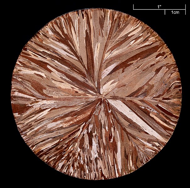
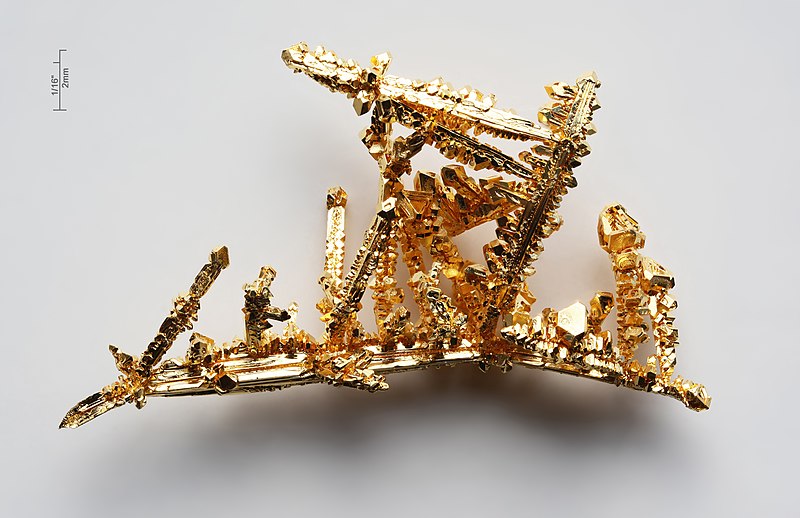
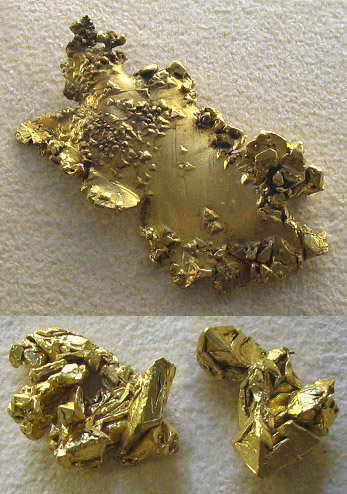
              One reason I bet is that all matter is a division of the sea we all are floating in. Although the matter has more dense transporter channels then air it is the matter that keeps the wave on frequency sort of like a filter. When the matter deviates from the pattern of density it creates shears or inclusions in the material which forms boundries in the matter. These boundries are very evident in pictures of acid etched metals which show two things. One that almost all matter has a crystaline pattern in them and that the boundries are merely density changes. I will show etched copper for instance here:


              And now iron:


              And now gold in it's natural formation:


              If there was no basic foundational particle smaller then we could see then how does phi work into your theory? Why would phi even be able to be applied to anything natural that grows? How can crystals grow in only one form separate from other crystals formation? Why are they not the same in every instance? Do you know that if we wanted to get a crystal to grow that we need a seed crystal or the crystal doesn't form in the method it should form in... Where does this seed come from in nature? Why does formation differ from region to region. There are a lot of questions that are not answered by your theory.

              Look at the iron sample picture really close and you can see a pattern there. Where did that come from. Iron itself is not a crystal it has a crystaline form which is much different. Where does that pattern originate from?

              This is a quote from the natural heading of the Golden ratio (Phi) on wikipedia:

              "Adolf Zeising, whose main interests were mathematics and philosophy, found the golden ratio expressed in the arrangement of branches along the stems of plants and of veins in leaves. He extended his research to the skeletons of animals and the branchings of their veins and nerves, to the proportions of chemical compounds and the geometry of crystals, even to the use of proportion in artistic endeavors. In these phenomena he saw the golden ratio operating as a universal law.[51] In connection with his scheme for golden-ratio-based human body proportions, Zeising wrote in 1854 of a universal law "in which is contained the ground-principle of all formative striving for beauty and completeness in the realms of both nature and art, and which permeates, as a paramount spiritual ideal, all structures, forms and proportions, whether cosmic or individual, organic or inorganic, acoustic or optical; which finds its fullest realization, however, in the human form."[52]
              In 2003, Volkmar Weiss and Harald Weiss analyzed psychometric data and theoretical considerations and concluded that the golden ratio underlies the clock cycle of brain waves.[53] In 2008 this was empirically confirmed by a group of neurobiologists.[54]
              In 2010, the journal Science reported that the golden ratio is present at the atomic scale in the magnetic resonance of spins in cobalt niobate crystals.[55]
              Several researchers have proposed connections between the golden ratio and human genome DNA."

              So here we have a fundamental occurrence in everything we look at. A law if you will of growth. it even resides on the most fundamental way that we think. So I put to you there is a fundamental particle. This particle is way smaller then the biggest atom smasher will ever be able to obtain. We quite possibly can never see it without the aid of computers but we sure can see the results of it. That was empirically proven more then once. How many times must we herald there is a fundamental rules set and accordingly particle that the rule set is locked into to make it a real law for all of nature to follow by virtue of it's matter.
              Last edited by Jbignes5; 11-08-2010, 07:56 PM.

              Comment


              • #37
                Originally posted by Goldfinder View Post
                To all you would be OUO researchers:
                Mass is aether trapped in a vortex. See - Besant and Leadbetter, Lucas and Bergman, Global Scaling, Stowe, and others. The only truly stable particles are the electron and the proton. The next most stable particle is the neutron which decays in seconds to an electron and proton. The neutron is obviously a proton and electron pressured together within the nucleus. The rest of the particle soup are just transitory decays of the initial stable particles.

                Electric fields are stresses in the field, Gravity is GRAD E, and magnetic fields are vortexes in the aether. EM energy are synchronous moving electric and magnetic fields.

                The proton and electron are resonant structures and tuned into the standing scalar waves as well as an infinitude of others. See Global Scaling. These structures of mass are already sustained and supported by the gravitational/scalar standing waves that run the universe. They are tapping the aether directly.

                Stifflers exciter is creating a disturbance in the aether and then taps this disturbance. So how does the tap work?

                After playing with the exciter and plowing through the tons of videos and associated work there is a great scarcity of anything other more variation of these circuits and no real discussion on HOW they are tapping the ZPE/aether/whatever.

                It looks to me in my limited background that the AV plug is really where the secret lies. The other thing is the transistor itself which seems to be limited to certain special ones. So what is common to AV plugs and transistors besides wire and containers - answer - semiconductor material...

                It reminds me when I was at Lockheed back in the 1960s. One of techs I who worked in the semi lab said they had been testing a transistor that put out energy with no inputs and it had gotten classified TS very quickly. He wouldn't discuss it further.

                When I met Dr. T. Henry Moray back on the early 1960s he showed me the progression of his radiant energy discoveries and how he went from giant Tesla towers outside his lab to a box that would fit into the trunk of a car to tap the aetheric forces that put out 100 KW. However, he stated that his greatest discovery was the use of semi conductor material. He was actually the first inventor to build a transistor and the device was stolen by Bell Labs.

                Space has this seething energy blazing through it. Various estimates go as high as 100 KW per cubic centimeter. The Dr. Stiffler exciters and other similar circuits tickle this standing wave field creating a disturbance in the aether and then trap the disturbance. Why not tap the seething field of energy directly? If the Lockheed free energy transistor and Dr. Moray's cryptic statement have some weight it looks to me the way to go. Not being a semiconductor expert (yes I have a number of the college courses on the material) maybe there is someone out there in lala land that could contribute.

                So if anyone else wants to contribute to this thread - lets have it !

                Goldfinder
                BTW mass particles, the whole of the periodic table are resonant structures in the aether.
                @Goldfinder

                Was the transistor of which you speak the 'Fogal Transistor'?

                http://blog.hasslberger.com/docs/CHA...TECHNOLOGY.pdf

                Comment


                • #38
                  Seed Structure

                  Hi Jbignes5,

                  If there was no basic foundational particle smaller then we could see then how does phi work into your theory? Why would phi even be able to be applied to anything natural that grows? How can crystals grow in only one form separate from other crystals formation? Why are they not the same in every instance? Do you know that if we wanted to get a crystal to grow that we need a seed crystal or the crystal doesn't form in the method it should form in... Where does this seed come from in nature? Why does formation differ from region to region. There are a lot of questions that are not answered by your theory.
                  The basic structure at the formation of all mass, is a geometrical shape of several dimensions. If you look at this diagram, in the middle there is a flattened diamond shape intersected by the equatorial divide, it is the shape of two cones connected at thier bases, one inverted. I think this is the basic buiding block of every thing. The forces surrounding it in the diagram serve to keep it stable through the continuous tapping of the Eather.


                  Well thats what I see anyway. If there is a basic partical, it is mass.

                  Quote:
                  " All mass is formed by a contraction of the electric poles of the generative cones of energy to the point of north of it's gravicative center and by an expansion of the contours of the radiative cones untill they disapear in the plane of the equator."
                  I think this definition is correct I wish somebody would tell me how they think mass is formed. That is where we need to start in my opinion.

                  If two people are searching a path and one starts at the begining one at the end when they pass in the middle the one that stated at the begining is making progress, the one that started at the end is backtracking.

                  Cheers
                  Last edited by Farmhand; 11-08-2010, 09:12 PM.

                  Comment


                  • #39
                    Originally posted by DrStiffler View Post
                    @Goldfinder

                    Was the transistor of which you speak the 'Fogal Transistor'?

                    http://blog.hasslberger.com/docs/CHA...TECHNOLOGY.pdf
                    Looks interesting, even though it appears hard to read.
                    More on this thing:

                    Index of /Physics/Scalar_Vector_Pot_And_Rick_Andersen
                    prodwav2

                    BEARDEN and the FOGAL TRANSISTOR PATENT

                    Lately (after 1995 or so) Tom Bearden has been busy with an inventor named Fogal, who has come up with a semiconductor device that allegedly "blocks charge" while allowing a "signal" to "tunnel", as it were, across a barrier; this sort of resembles a "communications"-oriented version of his 1993 Free Energy concept of a "degenerate semiconductor collector" which was supposed to "extract pure potential from a source, and switch it to a load, without drawing any current from the source"-- thus providing POWER to a load from POTENTIAL.

                    The idea here is that there is a "gap" isolating the power source from the load, and a "collector" device which alternately "scoops up" some "potential" from the source, then "feeds" it to the load; the source and load are never directly connected and the idea is that current is never allowed to flow -- just potential itself -- so the source never gets depleted and the load power comes from the "potentializing" and flowing of the free electrons already existing on the load side of the wiring and in the load itself. Orthodox engineers cringe at such "fantasies", but Fogal has apparently accomplished something similar:

                    Bearden has reported recently on Fogal's successful transmission and reception of a video signal, "hidden" (via scalar-EM/Fogal methodology) inside a DC voltage!!!

                    This reminded me of some of Bearden's earlier works which mentioned the possibility of "infolding" or piggybacking scalar signals-- hidden from normal detection-- onto "normal" EM carriers, such as the infamous "Woodpecker" over-the-horizon radars that the Soviets rattled the airwaves with for so many years. But now he is talking about folding up AC modulation inside DC!
                    The Bearden Free Energy Collector

                    So, according to Tom Bearden, for tapping Free Energy, the purpose is to charge a " Collector " during its relaxation time and then, to switch this Collector to a common resistive load, just before that the electrons begin to flow in the circuit.

                    << We took some trapped EM energy density (a chunk of potential gradient, a "voltage" before current flows) from the source, by switching that potential gradient (energy density, which is joules per coulomb) onto a collector (containing a certain number of coulombs of trapped charges) where the potential gradient activates/potentializes/couples-to these temporarily non translating electrons. So the finite collector collected a finite amount of excess energy [joules/coulomb x collecting (trapped) coulombs] on its now-excited (activated) free electrons. Then, before any current has yet flowed from the source, we switched that potentialized collector (with its temporarily restrained but potentialized electrons; with their finite amount of excess trapped EM energy) away from the source and directly across the load. Shortly thereafter, the relaxation time in the collector expires. The potentialized electrons in the collector are freed to move in the external load circuit, consisting of the collector and the load, and so they do so. >> has said Tom Bearden.

                    For the Collector it is necessary to use a conductive material which has a longer relaxation time than in the copper. This is only for the electronic circuit design and the limitation of its components. So, Tom Bearden has used " a Degenerate Semiconductor " which has a relaxation time of about 1 ms. The Collector is made with 98% Aluminum and 2% Iron.

                    << Degenerate semiconductor :

                    * A heavily doped semiconductor in which the Fermi level is located in either the valence band or the conduction band (see energy band ) causing the material to behave as a metal. >>

                    The Bearden's Collector is charged by using a Stepwise Charging method with a ramp voltage generator, this is commonly used in high efficiency and low power consumption CMOS systems which use an Adiabatic Charging method ( see Charge Recycling Clocking for Adiatbatic Style Logic by Luns Tee, Lizhen Zheng ). With this Stepwise Charging method very few energy is required for charging the Collector. If the Collector is a common capacitor the efficiency is nearly close to 100%. With the Bearden's Collector, this method is used only for transfering the potential. The ramp duration of the voltage must be less than the relaxation time of the Collector used. So, there is no current flow in the circuit ( dQ/dt ~ 0 ) during the charging sequence. When the Collector is fully charged, all the free electrons are "potentialized", they have their own kinetic energy gained by the potential only produced by the S-Flow. The next step is to use these "potentialized electrons "by switching the circuit on the Load, now, the Collector acts as a Free Source of Energy, it acts as a dipole energized by only the S-Flow of the original source...
                    A very fat critical report on this thing:
                    Comcast

                    Testing the Charged Barrier Transistor: A Personal Encounter with Pseudoscience - the story of my encounter with Bill Fogal and his charged barrier transistor. This 109 page document includes my technical report, copies of the letters I received from Bill Fogal and CTEC, and the cover letter from the latest set of test results that Mr. Fogal was distributing as of December 2006.
                    Update: looked quickly trough this report. I don't think this is what Goldfinder was referring to. The basic idea is to have a resistor in parallel with a tantanium capacitor as close to the emitter of the transistor as possible. Fogal's prototype consisted of a standard transistor, which he opened and soldered the emitter circuit on to using SMD components.

                    The test report describes testing this transistor in a standard circuit. If this thing is capable of doing something unusual, which might mean doing something with longitudinal electric waves, then you can't say much about this when you consider it as a normal transistor.

                    What is an interesting detail is that somewhere along the articles I scanned trough, it was said that it had to be an electrolytic capacitor. And under some circumstances these do act as diodes, namely when the dielectric layer breaks and you get a shortcut across the electrolyte.

                    If that were the case, then you get a non-linear device, which may be interesting in some cases, even though I don't see where or what at the moment.
                    Last edited by lamare; 11-08-2010, 09:55 PM.

                    Comment


                    • #40
                      Hi Jbignes5,


                      If there was no basic foundational particle smaller then we could see then how does phi work into your theory? Why would phi even be able to be applied to anything natural that grows? How can crystals grow in only one form separate from other crystals formation? Why are they not the same in every instance? Do you know that if we wanted to get a crystal to grow that we need a seed crystal or the crystal doesn't form in the method it should form in... Where does this seed come from in nature? Why does formation differ from region to region. There are a lot of questions that are not answered by your theory.
                      This theory fits perfectly into your work if you just replace the word "partical" with "structure".

                      The basic structure at the formation of all mass, is a geometrical shape of several dimensions. If you look at this diagram, in the middle there is a flattened diamond shape intersected by the equatorial divide, it is the shape of two cones connected at thier bases, one inverted. I think this is the basic buiding block of every thing. The forces surrounding it in the diagram serve to keep it stable through the continuous tapping of the Eather.
                      In my opinion it is a very neat fit. But what do I know. This basic structure is the universal shape or the shape of the universe. I believe it till someone can give me a better theory.

                      I don't even know what the textbooks say on this, can somebody fill me in on that, Please.

                      Regards

                      Comment


                      • #41
                        Hi Goldfinder,

                        You wrote.
                        And I think we agree we want some kind of Electric field to set up the tap. So lets look at semiconductor materials. I'll post something later today if I can get the time on this or someone else can take a stab at it and cobble together a summary of semiconductor materials, especially diodes.
                        The electric field already exsists. Dosen't it ?

                        Comment


                        • #42
                          Actually I may have made a small mistake the diamond I refer to is a field.

                          The diamond shape I mean is actually inside that and is tall not squat or flattened it's there if you look hard.

                          I can outline it.

                          Comment


                          • #43
                            Originally posted by Goldfinder View Post
                            And I agree, low frequency is one good possibility. One of my earliest success in tapping the aether was a signal of 128 Khz which I had derived from my visit w/ Dr. Moray. It was one of the base resonant frequencies in the Van Allen belts. Unfortunately, I can't find my old notes from 1960 where I had a precise derivation of the frequency.

                            Some of my intuits are that High Voltage is necessary. Tesla used HV, Dr. Moray used HV and claimed he got his stuff from discussions w/ Tesla back in the 1920s.
                            It depends on where you want to go. As far as I can tell, the basic principle of Tesla, Moray, Gray, Kapanadze and Stifflers circuits is to get a coil into higher harmonic resonance. The more higher harmonics you are able to get in there, the more energy you can tap from the dipoles in the coils, because the higher the frequencies you use, the more dipoles you get in the coil, of which you only have to drive one yourself.

                            In this line of thinking, the essential element of getting these high harmonics is (ultra) fast switching, so you get a very high bandwidth. Stiffler has found a specific transistor which can do that and the other ones use sparkgaps and HV. And both ways give you a very sharp rise (or drop) of the voltage you supply to the coil to keep it in resonance.

                            So, the essential key is: steep gradients in the circuit that steers the coil. Then you get these higher harmonics, which are benefitial, as far as I can tell.

                            However, you wanted to do to a semiconductor only solution, which is supposed to work without an external power supply. That would be a completely different beast, to say the least. If such a device is possible, it can only work if you tap an existing energy flow, such as the gradients in the E-field that cause gravity, or some other signal, like maybe what you refer to. However, even with signals in the kHz region, it seems you would need at least some kind of antenna and tuning circuit, which would be more than just one transistor or some other kind of layered semiconductor device.

                            To make a long story short: If you want to look for a single semiconductor device, you are looking for a completely different working principle. The only thing I can think of is that the gravity gradient may be somehow capable of giving you a voltage difference, that it can charge a capacitor, which could maybe be the capacitance across a PN junction. If that were the case, you wouldn't be able to measure this in a normal way, because you would get the same voltage difference across your probes, because they are experiencing the same field. However, if you could get a voltage difference across (a number of) PN juntion(s) this way, you would have an energy source you may be able to use.
                            Last edited by lamare; 11-08-2010, 10:22 PM.

                            Comment


                            • #44
                              Hows this,

                              This is what I wanted to showJbignes5.
                              [IMG][/IMG]

                              Here's how I think Otis made use of this, Maybe somehow.


                              Like this,

                              http://kobjxq.bay.livefilestore.com/..._sm.png?psid=1

                              There must be an easier way. Don't hold back folks.

                              This is interesting in the two small diagrams to the right the structure in the middle changes size, maybe when energy is removed and replaced.


                              I was going to try this in a counter rotating, Rotor/Stator arrangement with four electromagnets providing the EMF, the pulses to the electromagnets could be provided by switching the source of drive power with a single MOSFET. Bolted down of course.

                              Thats also off topic so I appologise.
                              Last edited by Farmhand; 11-21-2010, 06:45 AM.

                              Comment


                              • #45
                                Originally posted by Farmhand View Post
                                Hows this,

                                This is waht I wanted to showJbignes5.


                                Here's how I think Otis made use of this, Maybe somehow.


                                Like this,


                                There must be an easier way. Don't hold back folks.

                                This is interesting the structure in the middle changes size, maybe when energy is removed and replaced.


                                I was going to try this in a counter rotating, Rotor/Stator arrangement with four electromagnets providing the EMF, the pulses to the electromagnets could be provided by switching the source of drive power with a single MOSFET. Bolted down of course.

                                Thats also off topic so I appologise.
                                What if what you have there is two halves of the single particle. A half diamond would be two triangles base to base. The bases hold the charge that binds them and the focal point is the tips. This guides the waves or fields as you put it to radiate out from the base and get concentrated twords the tips. This would give the effect of a swirling field above the tips just like in the Great Pyramids.

                                I'm telling you they knew the fundamental shape of this particle. Who ever built the Great Pyramids knew way more and these were mere monuments to the smallest particle in existence that was responsible for all movement in the universe. It all fits.

                                I truely believe this is the most important fact and it would suggest that geometry in fields is very very important to both add and take away the power you need. Plus it has been proven that geometric coils like the Rodin coil produce more output then traditional coils. Tesla even states this with his conical coils.

                                Comment

                                Working...
                                X