MOSFET question
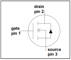
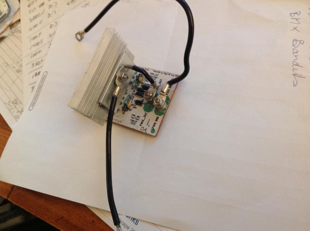
Assembling my OSHpark Monser driver v5.1 boards finally. On the MOSFET, Pin 1 is the gate, Pin 2 the drain and Pin 3 the source. What I am seeing seems a little counter intuitive, is that the "source" pin is hooked up to the board and battery ground then? Is my understanding correct? Here are the diagrams.
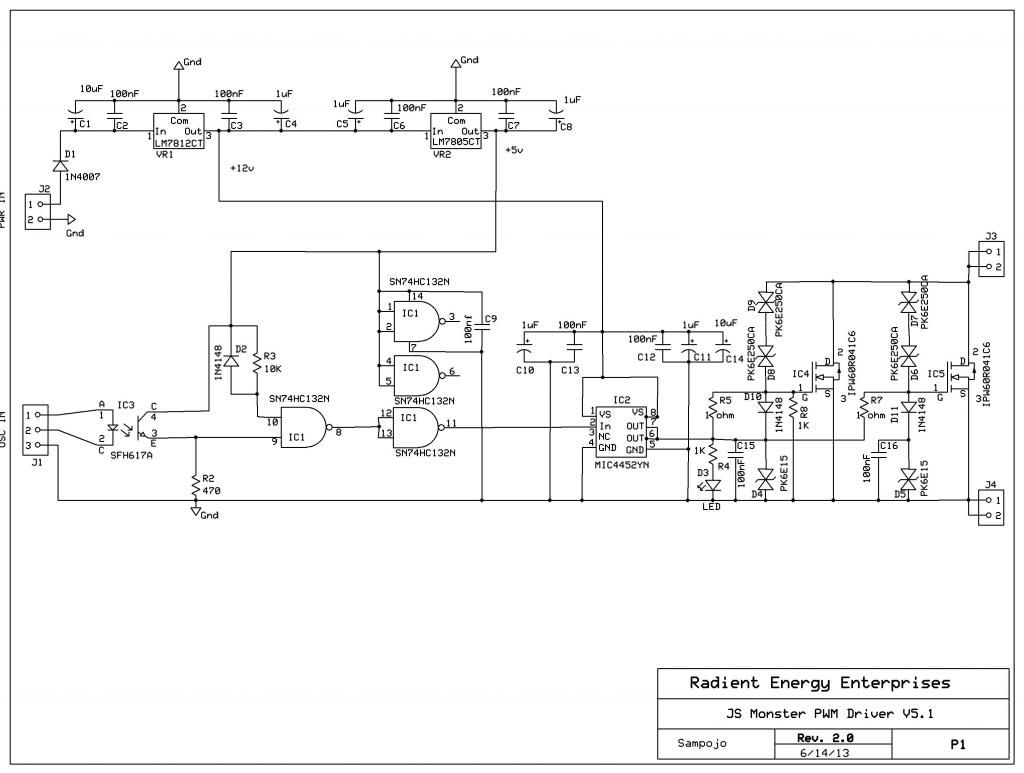
Schematic: (Note: R2 value is incorrect, has been changed to 330)

(This is now the corrected image, using blogspot instead of photobucket)
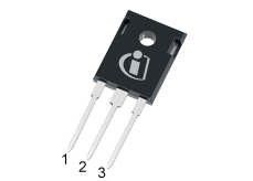
Package diagram

Piece schematic
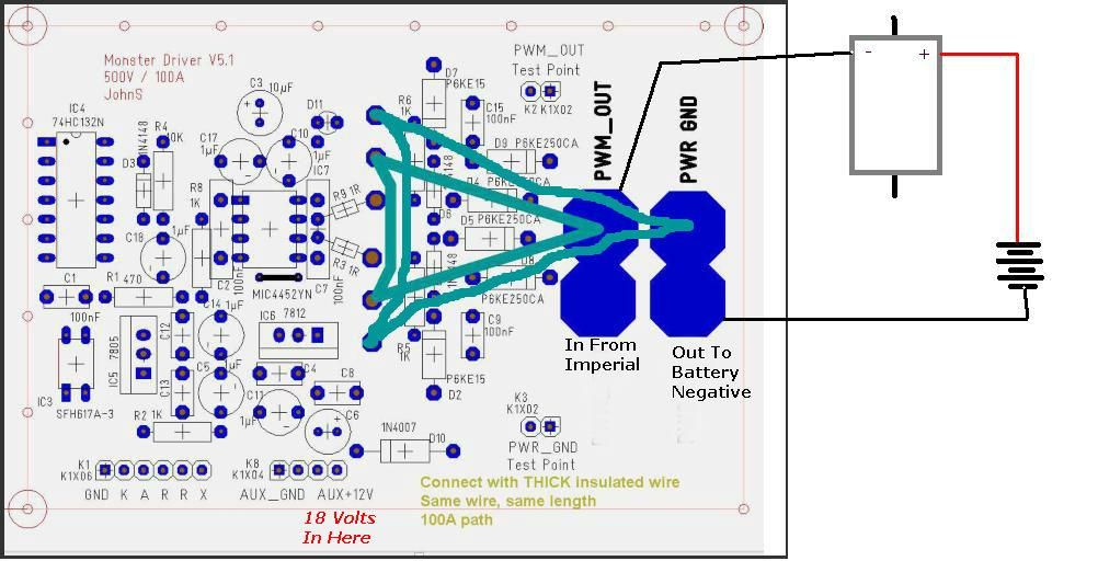
Using 1 ohm on R3,8 Edit: Sorry, threw up my old express PCB schematic, not numbered the same as JS T3001 schematic. It is R7,8 on this diagram and R3,9 on the JS schematic
Any input appreciated
Assembling my OSHpark Monser driver v5.1 boards finally. On the MOSFET, Pin 1 is the gate, Pin 2 the drain and Pin 3 the source. What I am seeing seems a little counter intuitive, is that the "source" pin is hooked up to the board and battery ground then? Is my understanding correct? Here are the diagrams.
Schematic: (Note: R2 value is incorrect, has been changed to 330)

(This is now the corrected image, using blogspot instead of photobucket)
Package diagram

Piece schematic

Using 1 ohm on R3,8 Edit: Sorry, threw up my old express PCB schematic, not numbered the same as JS T3001 schematic. It is R7,8 on this diagram and R3,9 on the JS schematic
Any input appreciated




Comment