Announcement

Collapse
No announcement yet.

More enormous proof of Dollard re: Dielectricity. beautiful videos!! MUST SEE!

Collapse
X
 
  • Filter
  • Time
  • Show
Clear All
new posts

  • More enormous proof of Dollard re: Dielectricity. beautiful videos!! MUST SEE!

    Must must see video!!!! Youll love it / them

    https://www.youtube.com/watch?v=9Po35g23fYI
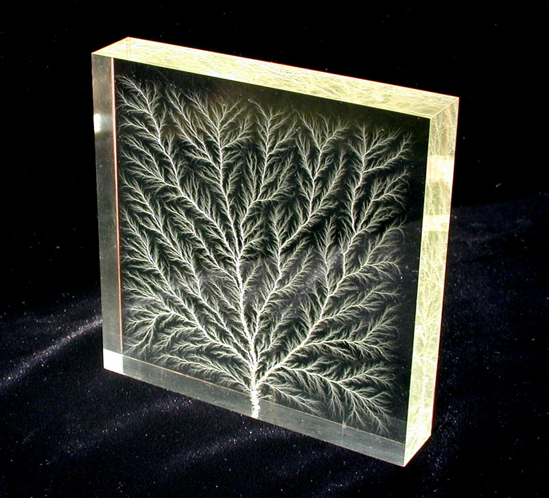


    he sells the sculptures on ebay for $40 a pop (the simple ones)

    unfortunately the demented SOB of this video call the discharges "electrons"


    which as any Dollard fan knows, there are NO electrons, its purely 100% dielectric discharges.


    Their IDIOT WEBSITE SAYS: "Since acrylic is an excellent electrical insulator, the huge charge became temporarily trapped, similar to the way electrically charged regions are temporarily trapped within thunderclouds prior to a lightning strike. "


    High Voltage Arcs and Sparks Page


    ARGHHHHHHHHH!!!!!!!!!!!


    Acrylic is an EXCELLENT DIELECTRIC CAPACITOR

    Theyre making wonderful scuptures but they dont even know the difference between electrical and electro-static/DIELECTRICITY!!!

    Tesla denied electrons were particles, so did Heaviside, so did CP Steinmetz!!!
    Last edited by TheoriaApophasis; 06-01-2014, 08:53 PM.

  • #2
    I actually talked to the SUPREME IDIOT that makes these things , the owner at Teslamania, Bert Hickman's site about Quarter Shrinking, Lichtenberg Figures, Tesla Coils, Nikola Tesla, Pulsed Power, and big Arcs and Sparks


    I mentioned Eric Dollard and he had a FIT, calling him a fool etc etc etc.


    He said he was actually charging the Plexiglass FULL OF ELECTRONS!!!


    Even his OWN &#*(#( website says:

    What are Lichtenberg Figures, and how are they Made?


    His website says: "Because acrylic is an excellent electrical insulator, injected electrons become temporarily trapped inside the acrylic"

    Duhhh, electrical insulators are DIELECTRIC CAPACITORS!!! Glass, Air, plexiglass, etc etc.

    website says: "the target material's dielectric properties"

    Yes, Dielectric CAPACITANCE , numbskull. My lord people are dumb!!!!

    He ignorantly thinks he is injecting electrons into the plexiglass!


    From his site:


    the target material's dielectric properties
    , and its atomic density. The higher the energy of the electron beam, the deeper the electrons will penetrate. For example, electrons with an energy of five MeV will penetrate about one-half inch through acrylic, but a sheet of lead only 1/16" thick will completely stop them.
    When a thick piece of acrylic is irradiated, huge numbers of electrons accumulate inside the specimen, creating a strongly-charged cloud-like layer called a space charge. Because acrylic is an excellent electrical insulator, injected electrons become temporarily trapped inside the acrylic. By passing specimens through the electron beam in two or more passes, changing specimen orientation between passes or rotating them while they're being irradiated, complex 3-dimensional space charge regions can be created. As the number of electrons accumulate during irradiation, the electrical stress (called the electrical field or "E-field") inside the acrylic dramatically rises, reaching several million volts per centimeter. We normally charge our specimens to just below the point where they'll break down. We then force the charged specimen to release ("discharge") the electrons at the desired location by poking it with a heavily-insulated, pointed metal tool. This creates a small fracture that concentrates the electrical stress at that point. The electrical field at the tip of the fracture overcomes the dielectric strength


    another moron! Little did he know I was about to spend a fortune with him on his artwork.


    Instead he talked to me like a DOG and was a smug elitist POS *@(()!!@@

    Comment


    • #3
      Dust Ferns

      Here is a photo of similar Fern-like patterns formed from settling dust inside the plastic case of some electronic equipment. Fern like patterns are formed when the dust settles inside a plastic case of this equipment. The fern like patterns are formed from dust which can be wiped away.


      Photo supplied from a friend who was curious as to what makes these patterns form. There were no significant HV supplies within the electronic device.

      I think during part of the LCD manufacturing process when they manufacture the plastic case, certain methods involving some kind of spot welder designed for plastic is employed. (You can see the patterns emerge out of the round circle welding spots). Some of the spot welding electrical energy is imprinted into the plastic on / around the weld. Since the plastic case medium is a good dielectric, it stores some of this imprinted dielectricity, within the plastic and it stays there, generally for good.* (See MIT dissectible capacitor demo etc.).* *

      So in my opinion as the dust settles within the housing over time, it is attracted to the dielectric charge imprinted within the plastic itself, (via a dielectric induction process during the manufacturing process). As the dust settles it aligns itself (dust is a dielectric too) which then maps out a pretty fern like patterns within the underlying plastic material. This is where the pattern originates from.

      Don’t be too concerned, they’re not idiots as such, it’s only their ignorance. - For some the mind virus is too far entrenched and they cannot be cured.

      Sputins
      Last edited by Sputins; 06-02-2014, 04:56 AM.
      "Doesn't matter how many times you kick the coyote in the head, it's still gonna eat chickens". - EPD

      Comment


      • #4
        just created this one:


        Haaaa!!!


        Comment


        • #5
          Originally posted by Sputins View Post
          Here is a photo of similar Fern-like patterns formed from settling dust inside the plastic case of some electronic equipment. Fern like patterns are formed when the dust settles inside a plastic case of this equipment. The fern like patterns are formed from dust which can be wiped away.


          Photo supplied from a friend who was curious as to what makes these patterns form. There were no significant HV supplies within the electronic device.

          I think during part of the LCD manufacturing process when they manufacture the plastic case, certain methods involving some kind of spot welder designed for plastic is employed. (You can see the patterns emerge out of the round circle welding spots). Some of the spot welding electrical energy is imprinted into the plastic on / around the weld. Since the plastic case medium is a good dielectric, it stores some of this imprinted dielectricity, within the plastic and it stays there, generally for good.* (See MIT dissectible capacitor demo etc.).* *

          So in my opinion as the dust settles within the housing over time, it is attracted to the dielectric charge imprinted within the plastic itself, (via a dielectric induction process during the manufacturing process). As the dust settles it aligns itself (dust is a dielectric too) which then maps out a pretty fern like patterns within the underlying plastic material. This is where the pattern originates from.

          Don’t be too concerned, they’re not idiots as such, it’s only their ignorance. - For some the mind virus is too far entrenched and they cannot be cured.

          Sputins
          Plastic is welded ultrasonicly.
          Ultrasonic welding - Wikipedia, the free encyclopedia

          Comment

          Working...
          X