Announcement

Collapse
No announcement yet.

COP 17 Heater | Rosemary Ainslie

Collapse
This topic is closed.
X
This is a sticky topic.
X
X
 
  • Filter
  • Time
  • Show
Clear All
new posts

  • @eternalightwithin,

    The heat sink is made by:

    Fischer Elektronik
    Type: SK 129/ 50,8/ STS
    Country: Germany
    Size: 55X43X25 mm

    f.cool

    The "extra hole" you are referring to is a plated through hole. Sometimes
    (when designing pcbs) one need to cross from the top layer on the board
    and to the bottom layer. (Or the opposite.)
    This is done to get an short wire from point a to point b.

    One also want to hide as many of those plated through hole as possible.
    So the usually way to do that is to hide the holes under components so that
    the holes is not visible when the components are soldered. If you look at the
    pcb you will see where that plated through hole goes.

    Also look at the design files found here: Index of /ufoufoufoufo
    (The Cadsoft Eagle CAD program is free and can be found on
    the Cadsoft site found here: CadSoft Online: EAGLE Layout Editor )

    On my site you can also find a very good temperature logger (TRS.rar).
    It handles -40 C to +85 C. There is also some other 555 timer projects there.

    If you have further questions, please ask, and I will try to answer them as
    best as I can.

    Oh, almost forgot, You must NOT use the parts values as shown on the
    pcb layout text. To get the correct duty cycle and frequency please use the
    parts described in the updated circuit drawing (http://home.no/ufoufoufoufo/anc_revB_sch.gif) found on my site.

    Regards,
    Groundloop.
    Last edited by Groundloop; 09-25-2009, 06:15 AM.

    Comment


    • yes, that's it.

      Groundloop, Yes I know. Using Aaron's August 26 circuit. Also, why did you put 1N4004 in instead of just all 1n4148's ?

      And where did you get those awesome PCB mounts for wire attaching?


      Originally posted by FuzzyTomCat View Post
      Hi David,

      Do you have this Groundloops Assembled PCB Image

      Groundloop made the board so him or gotoluc would know where to get the heat sink maybe another member that got one 
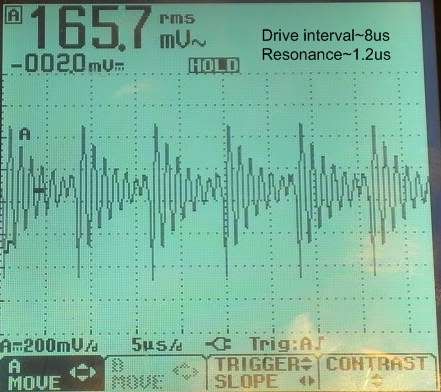
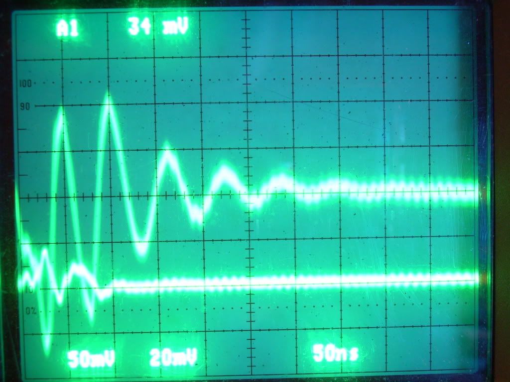
..... but the Mosfet seems not to get over 140 degrees F ever that I've seen with a heat sink like I have.

      Glen
      Last edited by eternalightwithin; 09-25-2009, 06:41 PM.

      Comment


      • Originally posted by eternalightwithin View Post
        yes, that's it.

        Groundloop, Yes I know. Using Aaron's August 26 circuit. Also, why did you put 1N4004 in instead of just all 1n4148's ?

        And where did you get those awesome PCB mounts for wire attaching?
        They look like Keystone Style Terminals

        Possibly available from Digi-key or Newark

        "Amy Pond, there is something you need to understand, and someday your life may depend on it: I am definitely a madman with a box." ~The Doctor

        Comment


        • @eternalightwithin,

          The 1N4004 is there to block the power to the 555 in case the operator
          connects the polarity the wrong way around. I was not sure how much
          power (read milli amps) the 555 was to use, so I played for safety and
          used a 1N4004 since this is an 1 ampere type. The 1N4148 is a low 200mA
          type. But if the 555 circuit uses less than 200mA then it is safe to use
          the 1N4148 all around.

          The pcb edge connectors are made by Phoenix. See this link:
          PHOENIX CONTACT | 1725656 MPT 0,5/ 2-2,54

          The small one are 2,54mm raster and the big one are 5mm raster.

          BTW: Did change the parts on my board to new values. Now the circuit
          perform OK. I can get the correct low duty cycle at the correct freq.
          Did a test today where I connected a HUGE 500 Watt transformer
          to the switch. I then connected the transformer (230VAC) output via
          a BY255 and back to the battery in a looped self powered configuration.
          The battery did loose charge at a linear manner so the circuit was
          not >COP 1. But it was a fun test. :-)


          Regards,
          Groundloop.

          Comment


          • Hi everyone,

            I thought I would post a interesting development that poynt99 had accomplished a actual spice close simulation of my wave form from the latest test. I must say that this phenomenon the "Negative Dominate" I've been looking at since the beginning of my postings of wave forms, from all my prior testing and only a few were actually aware of the significance. The wave forms shown are all from the standard 555 Power Adjustment potentiometer resistance rating of 1k to the last test having to use a additional 4K resistor because possibly of the usage of my 10 ohm "Quantum" prototype load resistor. ( see test data for actual 555 potentiometer resistance settings )

            Claimed OU circuit of Rosemary Ainslie


            All my four tests posted wave forms from the newest testing to the oldest -


            Thanks .99 for you hard work on this simulation ....

            Glen
            Last edited by FuzzyTomCat; 09-27-2009, 04:22 PM. Reason: additional information - 1K pot - .99 additions
            Open Source Experimentalist
            Open Source Research and Development

            Comment


            • This is somewhat out of sequence - and a bit off topic, but I feel there is a relationship between the RF cooling effects claimed by Aaron and these experiments.

              1047 & 1048 are the most dramatic:

              Experimental Physicist John Hutchison Freezes Water Using RF:
              1045

              1046

              1047

              1048

              1049

              1050

              1051

              1052

              FWIW

              "Amy Pond, there is something you need to understand, and someday your life may depend on it: I am definitely a madman with a box." ~The Doctor

              Comment


              • Fuzzy, .99 - good teamwork on the negative pulse stuff

                Correct me if I'm wrong, but are we not looking at the Source pin of the FET there? If so, isn't that negative spike related to the FET turning off? There is nothing to prohibit a negative potential on the drain from being transferred to the source. We would not see the initial positive there because it is blocked by the body diode and low off-state transconductance of the FET.

                Essentially, during this period, your reference, B(-), is in a positive position relative to the source of the FET. Therefore a negative current is flowing into the source pin. This gives you a negative voltage drop across the measurement resistor - aka 'shunt'.

                Can we see this waveform superimposed with the drain waveform for timing comparison?

                Cheers,

                "Amy Pond, there is something you need to understand, and someday your life may depend on it: I am definitely a madman with a box." ~The Doctor

                Comment


                • Hi Harvey - thanks for the JH clips. Strange man - and weird videos. He's got to be a magus. Can't help feeling he needs to do some serious housekeeping. What a trip.

                  Not that happy with the easy dismissal of the negative preceding the positive - but nor do I know enough to argue. To me the initial positive should be evident - somewhere. Are you seriously suggesting that it was 'snubbed' out by the body diode? Surely the body diode would have been bypassed? in that first discharge from the battery?

                  Comment


                  • Originally posted by witsend View Post
                    Hi Harvey - thanks for the JH clips. Strange man - and weird videos. He's got to be a magus. Can't help feeling he needs to do some serious housekeeping. What a trip.

                    Not that happy with the easy dismissal of the negative preceding the positive - but nor do I know enough to argue. To me the initial positive should be evident - somewhere. Are you seriously suggesting that it was 'snubbed' out by the body diode? Surely the body diode would have been bypassed? in that first discharge from the battery?

                    I can only guess based on the presentations. In an earlier post, Glen stated that his probe was on the Source pin, which is effectively across the current sensing resistor (aka shunt) tied to B(-). So we need to ask ourselves what condition produces a negative potential at that node relative to B(-).

                    Two Possible answers:

                    1: Source pin is being driven down in potential by a negative going pulse on the drain.

                    2: B(-) is being driven up by a positive going pulse on the drain (through the battery itself)

                    Either way, the energy is coming from the inductor. It has either been stored there during the on time charge up, or the spike opens a door to allow it to escape from some other storehouse e.g. Dirac's Sea.

                    During this period, the Battery is no longer the active energy source but instead the inductor takes over as the active source.

                    In the case of an inductor arranged properly to resonate with extant EM wave energy external to the circuit, extra energy can enter the circuit as it is subtracted from the external wave. There are very few EM waves occurring naturally capable of summing up 19W of average energy. That is the same as saying 380W for 20µs every 400µs.

                    Now a little simple math: 24V * 6.1A = 146.4W during on-time within continuous operating parameters of the IRFPG50. Not enough to reach the 380W needed. Also, I was being generous with the 20µs as the actual on-time pulse width is a bit over 15µs for 3.7% duty cycle at 2.4kHz. So really, at this periodic mode, we would need even more than 380W during the on-time to average the 19W needed to give COP > 17 with a 'shunt' measurement of 1.13W. Can we push the IRFPG50 beyond its 6.1A max? Yes, because that is the continuous current. This device can handle 24A pulsed and is only limited by the junction temperature. The Thermal Response curve flat-lines around 200ms with 50% duty cycle (Fig 11 in the Designers Guide for this part). Since we are well below that at 20µs we could drive the system up to 24A, or 576W without risk of failure. To put it in simple terms for everyone to understand, we can drive a 380W 24V lamp with this circuit at 3.7% Duty cycle, 2.4kHz and expect a 19W average - periodic operation ... if ... by some miracle, we could reduce the FET internal resistance to zero and have our lamp filament resistance set at 1.52 Ohms.

                    The short version of this is that we cannot get 19W with that time base with these parts. We must increase the number of times our transistor is on, and this is done by stealing from the off-time. So the on-time pulse width is maintained, but we effectively increase the duty cycle. This does naturally happen during aperiodic action, but we would expect the 'shunt' to reflect the increase in power consumption.

                    My next post will address some of the findings from my requested test on Aaron's circuit with Glen's Resistor.

                    "Amy Pond, there is something you need to understand, and someday your life may depend on it: I am definitely a madman with a box." ~The Doctor

                    Comment


                    • Thanks Harvey.

                      Comment


                      • Originally posted by Harvey View Post
                        Fuzzy, .99 - good teamwork on the negative pulse stuff

                        Correct me if I'm wrong, but are we not looking at the Source pin of the FET there?
                        Hi Harvey,

                        Thanks for your continued input .... Yes your correct that all scope images do show a probe connection between the mosfet source pin and the .25 ohm shunt ...... with slight differences between tests ...

                        Tektronix 2445A
                        Channel 1 (A1) ground is on battery negative side of shunt and probe is at 555 negative rail side of shunt. [20mV] [x10]
                        Channel 2 (A2) ground is on battery negative side of shunt and probe is at mosfet source side of shunt. [50mV] [x10]

                        Tektronix TDS 3054C
                        Channel 1 ground is on battery negative side of shunt and probe is at 555 negative rail side of shunt.
                        Channel 2 ground is on battery negative side of shunt and probe is at mosfet source side of shunt.


                        POST #2238
                        Ainslie - Murakami Negitive Dominant Waveform Generator (revised 08-26-09)

                        • Gate resistance: 53 ohms
                        • On pot resistance: 32.8 ohms
                        • Off pot resistance: 293.9 ohms
                        • NE555N power adjustment pot resistance: 93.1 ohms

                        Load Resistor - 10 ohm 100 watt "Memcor"


                        POST #2542
                        Ainslie - Murakami Negitive Dominant Waveform Generator (revised 09-11-09)

                        • Gate resistance: ? ohms ( 40 - 100 ohms estimated )
                        • On pot resistance: 32.8 ohms
                        • Off pot resistance: 293.9 ohms
                        • NE555N power adjustment pot resistance: 193.1 ohms

                        Load Resistor - 10 ohm 100 watt "Memcor"


                        POST #2606
                        Ainslie - Murakami Negitive Dominant Waveform Generator (revised 09-11-09)

                        • Gate resistance: 340.5 ohms
                        • On pot resistance: 63.1 ohms
                        • Off pot resistance: 689 ohms
                        • NE555N power adjustment pot resistance: 159.5 ohms

                        Load Resistor - 10 ohm 100 watt "Memcor"


                        POST #2764
                        Ainslie - Murakami Negitive Dominant Waveform Generator (revised 09-11-09)

                        • Gate resistance: ? ohms
                        • On pot resistance: ? ohms
                        • Off pot resistance: ? ohms
                        • NE555N power adjustment pot resistance: ? ohms

                        Load Resister - 10 ohm "Clarostat" 225 watt, 64.7 uH (Aaron's Original Test Load Resister)

                        2us Original (CSV file)
                        2us Crunched (CSV file)

                        (50 mV Div, 2us)


                        POST #2766
                        Ainslie - Murakami Negitive Dominant Waveform Generator (revised 09-11-09)

                        • Gate resistance: .5 ohms
                        • On pot resistance: 201.6 ohms
                        • Off pot resistance: 317.3 ohms
                        • NE555N power adjustment pot resistance: 688.0 ohms ( "plus" 4,000 ohm resister "Total" = 4,688.0 ohms )

                        Load Resistor - Prototype "Quantum" 10 Ohm "Replication"

                        20us Original (CSV file)
                        20us Crunched (CSV file)
                        2us Original (CSV file)
                        2us Crunched (CSV file)


                        Hope this clarify's all the "posted" testing that I have done and the changes between them.

                        Glen
                        Last edited by FuzzyTomCat; 09-27-2009, 04:25 AM. Reason: general correction info - Post #2542
                        Open Source Experimentalist
                        Open Source Research and Development

                        Comment


                        • Originally posted by Harvey View Post

                          Can we see this waveform superimposed with the drain waveform for timing comparison?
                          Hi Harvey,

                          Sorry I missed this the first time was kinda busy at the time ..... I'll see what I can do .... I'm still in the process of trying to make a replacement "Quantum" prototype resistor for testing and only have my 10 ohm 100 watt "Memcor" plus not a TDS 3054C for any trick stuff just my Tek 2445A .....

                          Glen
                          Open Source Experimentalist
                          Open Source Research and Development

                          Comment


                          • winding direction

                            Hi Glen,

                            Do you plan on making a couple resistors that are wound in both directions? Might be interesting to see if that shows any difference on the scope. The one you left with me is wound for South at the end where the positive is.

                            Hard to tell what all these ceramic ones are - can't make out the direction of the winding where they come out to the tab.

                            I guess I could stick an iron core in them, charge it up and see which polarity the core charges at and that should tell me.
                            Sincerely,
                            Aaron Murakami

                            Books & Videos https://emediapress.com
                            Conference http://energyscienceconference.com
                            RPX & MWO http://vril.io

                            Comment


                            • Larger Pic

                              Larger Pic

                              It was determined that there is an unknown component in the Radio-Location Bands above 3GHz present in the 'noise' and sufficient to intrude on the data. This signal was present even with the power stage inoperable. The source of this signal is yet to be determined. It may be finding its way into the circuit from the scope ground system.

                              The test configuration used is presented above and organized in such a way so as to reveal any breakdown in KCL. The operation was Aperiodic. The resistor used was Glen's, documented elsewhere. I was not concerned with the circuit timing or the components used for the timer, as this test was aimed at the aperiodic operation and its effects on the current flow in the circuit. The CSR (current sensing resistors) are all 0.25 Ohm 5%. Therefore I charted a minimum and a maximum value for the current in each leg of the circuit.

                              The instantaneous voltage at CH1 was used for power calculations for each leg based on the Max current (min tolerance resistance value). The absolute value of that current was used. Thus all of the power values are above zero for all three legs.

                              The sum of the timer leg and load leg were compared to the B(+) leg and the 'missing' value was charted. The 'missing' instantaneous current ranged from +285mA to -305mA and may be directly related to the unknown signal. However, there is a clear indication of positive current flow through the B(+) leg at that point in time that a negative current flow exists in the load leg. The value of this event appears to be greater than the maximum recorded amplitude of the noise present, but we must realize the the scope used and the samples taken may be inadequate for GHz signals - although it did register that frequency according to Aaron.

                              Because of the very aperiodic data, I did calculate the average power for each leg to get a better overall picture using the technique mentioned above. The average timer power was 316mW. The average power for the load was 410mW. The average power for the B(+) leg was 3.5W. The instantaneous power is charted above. Note that the timer and load show the bursts while the B(+) is constant.

                              I did try to look for inductive delays and shifted current, but the data makes this almost impossible.

                              I would like to revisit this test when the unknown energy component is discovered and dealt with. We cannot overlook the possibility that it may be coming from the battery or 'noisy' sensing resistors, or an interaction between the two.

                              At first glance, it appears that this circuit is taking power from the B(+) leg and returning it to the B(-) leg by some other path. This path can be RF, thermal or some other form of energy exchange otherwise undocumented as of yet. Or it could be and exchange with another energy pool. It definitely warrants deeper analysis and study.

                              "Amy Pond, there is something you need to understand, and someday your life may depend on it: I am definitely a madman with a box." ~The Doctor

                              Comment


                              • Not sure how appropriate this is - but was wondering if the initial phase of Fuzzy's waveform went positive. Then the resonating frequency gradually transferred to the resistor?

                                Alternatively, could it be that silicone - glass crystals - being pure - also have more latent energy than is conventionally assumed. Therefore, in terms of the model? - perhaps the glass will get cloudy - over time. Just a thought.


                                EDIT - Harvey - many thanks for the report. Have just read it. This is really interesting.
                                Last edited by witsend; 09-27-2009, 09:09 AM.

                                Comment

                                Working...
                                X